Best of the
Best
Editors' picks and our top buying guides


Best of the
Best
Editors' picks and our top buying guides
Latest

Huawei's New Phones Rely on More China-Made Parts
15 minutes ago
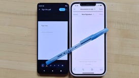
How to Take a Screenshot on Any iPhone or Android Phone
48 minutes ago
How to Watch 'Interview With the Vampire' Season 2 From Anywhere
48 minutes ago
Best Internet Deals for Seniors
48 minutes ago
Refinance Rates Slide Down Again: Refinance Rates for May 10, 2024
1 hour ago
22 Best High School Graduation Gifts for the Class of 2024
1 hour ago
iOS 17: Add More Security to Your iPhone Messages in 4 Easy Steps
1 hour ago
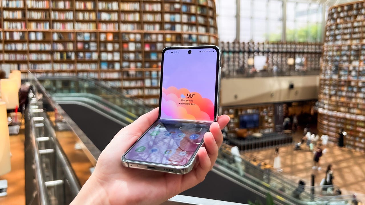
Best Android Phone of 2024
2 hours ago
Best CD Rates Today - High APYs Won't Stick Around Forever, May 10, 2024
2 hours ago
I Tried Gemini AI to Plan Mother's Day Last-Minute. It Took a Weird Turn
2 hours ago
Best Savings Rates Today -- Now's the Time to Take Advantage of APYs up to 5.55%, May 10, 2024
2 hours ago
My Favorite Espresso Machine Is Just $110 Right Now
3 hours ago
Give Mom the Gift of Perfectly Cooked Food This Mother's Day With This Ninja Air Fryer
3 hours ago
Today's NYT Connections Hints and Answers: Help for May 10, #334
8 hours ago
Today's Wordle Hints and Answer: Help for May 10, #1056
8 hours agoMore to Explore
Reviews, advice and more from CNET's experts.


Get the best price on everything CNET Shopping helps you get the best prices on your favorite products. Get promo codes and discounts with a single click.
Add to Chrome - it's free!
Our Expertise
Expertise Lindsey Turrentine is executive vice president for content and audience. She has helped shape digital media since digital media was born.
0357911176
02468104
024681025
Tech


Upgrade your inbox
Get CNET Insider
From talking fridges to iPhones, our experts are here to help make the world a little less complicated.
Money


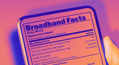
Crossing the Broadband Divide
Millions of Americans lack access to high-speed internet. Here's how to fix that.


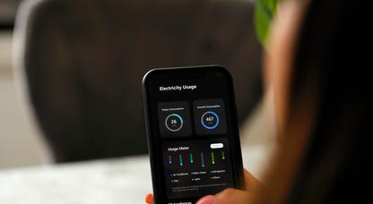
Energy and Utilities


Deep Dives
Immerse yourself in our in-depth stories.


Get the best price on everything CNET Shopping helps you get the best prices on your favorite products. Get promo codes and discounts with a single click.
Add to Chrome - it's free!
Internet


Sleep Through the Night
Get the best sleep of your life with our expert tips.


Get the best price on everything CNET Shopping helps you get the best prices on your favorite products. Get promo codes and discounts with a single click.
Add to Chrome - it's free!
Tech Tips
Get the most out of your phone with this expert advice.


Get the best price on everything CNET Shopping helps you get the best prices on your favorite products. Get promo codes and discounts with a single click.
Add to Chrome - it's free!

Home


Living Off Grid
CNET's Eric Mack has lived off the grid for over three years. Here's what he learned.