Best of the
Best
Editors' picks and our top buying guides


Best of the
Best
Editors' picks and our top buying guides
Latest

Best Budget 3D Printer of 2024
15 minutes ago
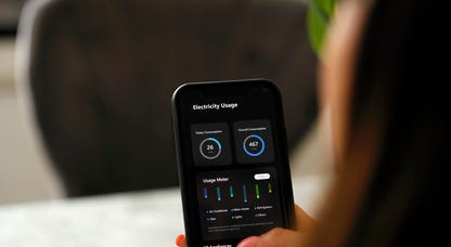
How to Shop and Compare Electricity Rates in Connecticut
1 hour agoFCC Reportedly Approves T-Mobile's Deal to Purchase Mint Mobile
1 hour ago
Best 4K TV Deals: Save Up to $1,000 on Top TVs From Samsung, LG and More
1 hour ago
Netflix Keeps Crashing on Roku TV
1 hour ago
Best Internet Providers in Cambridge, Massachusetts
2 hours ago
Best Twin Mattress for 2024
2 hours ago
NFL Draft 2024: How to Watch Tonight, Full Weekend TV Schedule, First Round Order
2 hours ago
Best iPhone 15 Deals: Get One Free With a Trade-In or New Line
3 hours ago
Best Bluetooth Speaker for 2024
3 hours ago
NBA Playoffs 2024: How to Watch Tonight's Games, Schedule, Matchups, TV Times
3 hours agoThreads Finally Lets You Mute Certain Words From Your Feed. Here's How
3 hours ago
Google Meet Is Making It Easier to Switch Between Devices
3 hours ago
Best Cheap TV Deals: Nab Fire TV, Roku, TCL and More for Less
4 hours ago
Forget Interest Rate Cuts. One Economist Says Rate Hikes Are More Likely This Year
4 hours agoMore to Explore
Reviews, advice and more from CNET's experts.


Get the best price on everything CNET Shopping helps you get the best prices on your favorite products. Get promo codes and discounts with a single click.
Add to Chrome - it's free!
Our Expertise
Expertise Lindsey Turrentine is executive vice president for content and audience. She has helped shape digital media since digital media was born.
0357911176
02468104
024681024
Featured in
Tech


Upgrade your inbox
Get CNET Insider
From talking fridges to iPhones, our experts are here to help make the world a little less complicated.
Featured in
Money


Crossing the Broadband Divide
Millions of Americans lack access to high-speed internet. Here's how to fix that.


Featured in
Energy and Utilities


Deep Dives
Immerse yourself in our in-depth stories.


Get the best price on everything CNET Shopping helps you get the best prices on your favorite products. Get promo codes and discounts with a single click.
Add to Chrome - it's free!
Featured in
Internet


Sleep Through the Night
Get the best sleep of your life with our expert tips.


Get the best price on everything CNET Shopping helps you get the best prices on your favorite products. Get promo codes and discounts with a single click.
Add to Chrome - it's free!
Tech Tips
Get the most out of your phone with this expert advice.


Get the best price on everything CNET Shopping helps you get the best prices on your favorite products. Get promo codes and discounts with a single click.
Add to Chrome - it's free!

Featured in
Home


Living Off Grid
CNET's Eric Mack has lived off the grid for over three years. Here's what he learned.