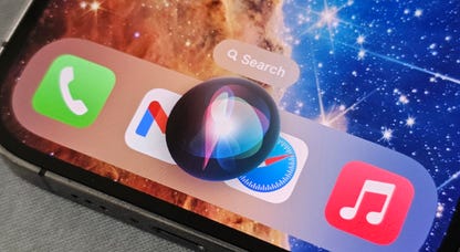
Commentary: AirPods have always received useful features with software updates. With iOS 18 around the corner, will AirPods get another hearing health option?
A new plant system fortified with microbiomes is engineered to clean as many toxins from your home's air as 30 normal plants.
AI will probably take center stage once again at the company's developer conference next month.
The tech giant has been conspicuously absent from the generative AI race so far.
New grants for Solar for All programs aim to install solar panels and boost community solar access nationwide. Here's the list of grantees near you.
All those trendy new AI tools make it easier to distort political narratives. You'll need to be on guard.
Surprise even the pickiest people on your list with these unique and useful gifts.
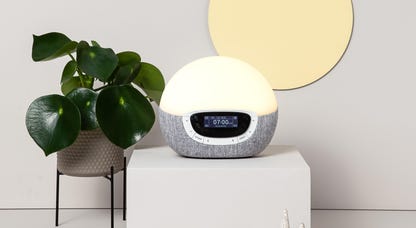
Sunrise alarm clocks slowly wake you up without any sudden, annoying sounds. Here are our picks of the best sunrise alarm clocks on the market.
Commentary: If you want to cultivate a work-and-travel lifestyle, you need the right gear without being bogged down. Here's what I bring.
You don't need to spend a fortune to show your mom just how much you love her. Here are some affordable Mother's Day gift options.
Commentary: The singer-songwriter has written yet another set of memorable new tracks for her latest album.
Kids aged 9 to 12 can be difficult to shop for, so we're here to help take the hassle out of finding the best gifts for tweens.
The dark anime series with John Wick vibes is closing out its first installment.
A white noise machine can lull you into a deep and restorative rest. Sleep soundly with one from our tried and tested best list.
Not on a strict budget? Here are some gift ideas for $300 or less that are sure to impress.
Whether you're an avid camper or have family in town, air beds are a go-to option. We tested and selected the best air mattresses on the market.
Here are all the hottest rumors surrounding the next major version of Apple's software.
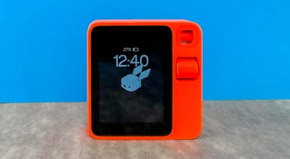
The Rabbit R1 can answer questions, play Spotify and record voice memos. But on my first day with it, the camera intrigued me the most.
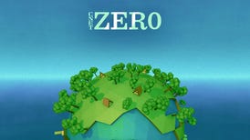
Everything you need to know about sustainability.
Learn to better navigate our digital world.
A dive into the infinite complexities.
The next stage in the internet's evolution.
Creating independence for everyone.